Measuring the Nearly Immeasurable

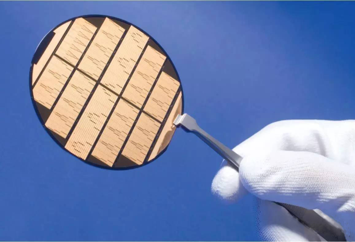
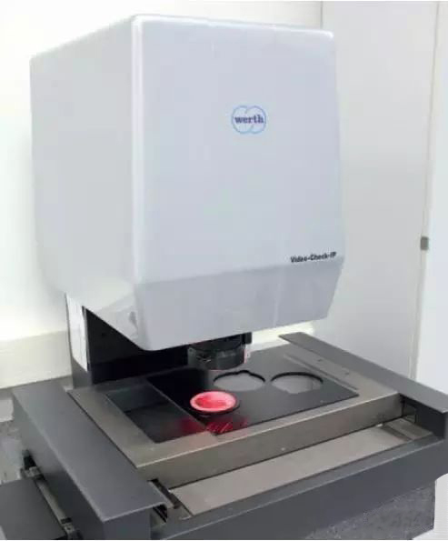
Incredible wafer thickness measurement the semiconductor laser and high frequency amplifier wafers produced at the Ferdinand Braun Institute in Berlin must reach an extremely precise layer thickness. Cleanroom workers use Werth multi-sensor coordinate measuring machines to monitor this process. The machine is equipped with a color difference sensor to accurately capture the required measurement elements without contact. Ferdinand Braun Institute and Leibniz Institute in Berlin. There are 220 employees, including 110 scientists. Development and production of materials processing, and precision measurement technology, as well as other diode laser products. The other is the production of high-frequency parts of communication technology, power electronics technology and sensors. 'The semiconductor laser has low mounting height and high-precision polishing and contact force,' said Dr. Andreas thies of the process technology department. Although such a laser is not larger than a grain of rice, it can output continuous wave operation of up to 20 watts or fast pulse wave of 100 watts. The of laser in optical disc is about 5000 to 25000 times. These characteristics, accompanied by high reliability under extreme conditions, make FBH laser famous all over the world. They even test atomic clocks in outer space, for example, in the next generation of GPS satellites. There are many applications in optics. In medical technology, they helped Zhiliao's photodynamic therapy by turning on an accurately defined wavelength and affected damaged cells and establishing 'Yaowu' in 'Zhongliu' cells. Further applications include optical precision measurement, Industrial measurement and material processing (bonding, welding and engraving). Various wafer processing processes, research and development of microwave technology and Optoelectronics are completed on the basis of basic technology (a single crystal semiconductor layer placed on the bottom of the single crystal) and the characteristic materials of the required extremely thin layer are assembled on the silicon wafer. Using modern technology, the wafer needs further processing. The processing process includes photolithography, wet and dry etching processes and metallization steps. About 2000 pieces and microwave circuits, or 10000 laser chips, can be assembled into 4-inch wafers. Incredible Wafer thickness measurement Figure 1 in the clean room: employees use 3D multi-sensor coordinate measuring machine and chromatographic focusing sensor to measure wafer thickness. Before technicians separate chips from wafers and assemble them into photoelectric or high-frequency components, wafers must be thin enough. To do this, they adhere to carrier materials, It is then ground and polished to a defined size. Dr. Andreas thies is a process technology expert at FBH and is responsible for clean room work. He explained that 'wafer thickness is an important indicator of component availability. As a rule, the wafer is under the bottom surface from the initial thickness of 350 μ M to 100 as little as possible μ m. According to different applications. Gallium arsenide (GaAs) or gallium nitride (GAN) made of 4-inch wafer is a necessary material for high-frequency applications. It is gallium arsenide for about two hours and gallium nitride for a longer time. To achieve the accurate target thickness, the wafer must be measured many times. Until recently, the measurement of this process was contact measurement. This method works by measuring the thickness of the wafer before it is adhered to a carrier. After gluing, it is measured again, and the difference between the two measured values can be used to approximate the layer thickness. This is used to calculate the thickness of the wafer after the raw material has been removed and ground. Because this method is not particularly accurate, the responsible parties decided to buy a special measuring machine, which will provide accurate results and work without contact as much as possible. Their choice is a videocheck 400x200x2003d-cnc, With chromatographic focusing probe (CFP) (Figure 1). This 3dcnc multi-sensor coordinate measuring machine from Werth measurement technology is accurate due to its unique pre installed operating system. The concept of this videocheck series of devices allows the combination of various sensors for corresponding applications (Fig. 2). In addition to the image processing sensor included in the basic version, various mechanical accessories, contact probe system, 3D optical fiber probe sensor, distance sensor, laser sensor, etc. can be integrated into the chromatographic focusing sensor - a complete set of chromatographic focusing probes are used to measure the wafer thickness. It is specially developed to accurately measure the non-contact, shiny, Reflective and transparent materials. Therefore, the sensor is particularly suitable for optical elements, such as mirrors and lenses. Capable of measuring semiconductors, such as wafers that are usually not transparent to white light, using special variants in the infrared range, Its light can penetrate semiconductor materials (Figure 3). The physical influence of each boundary surface at the boundary of the material produces interference, which will be used to calculate the wafer layer thickness. The key advantage of this sensor is that it measures the wafer material accurately and ignores the adhesive layer, metal layer, and front electrical structure. 'Dr. Andreas thies explains. The incredible wafer thickness measurement can be quickly established and implemented that 's ok. The engineer first places the wafer to be tested on the fixed clamping device on the X-Y workbench. Then use the winwerth measurement software in the computer to select the appropriate location and input the required basic information about the size and wafer material.

Figure 1 in the clean room: employees use 3D multi-sensor coordinate measuring machine and chromatographic focusing sensor to measure wafer thickness

Dr. Andreas thies said more accurately, 'we can measure gallium arsenide, gallium nitride, sapphire, silicon, silicon carbide. These are our main materials. For other materials, we can enter the refractive index. Enter the approximate thickness of the measured sample (estimated size is 50) μ m)。 In order to speed up the measurement speed, the current operator only needs to press start, and the machine starts the measurement process. The sensor scans the wafer in two directions through 'Zhongxin', one from the X direction and one from the Y direction. Each time the sensor detects, it is displayed on the screen to measure the wafer layer thickness. The workers found that it could actually analyze data directly in the PC on the device. Using the written program, the layer thickness distribution is calculated and displayed graphically. It takes about 2 minutes to measure a 70mm wafer. The user can see an accurate wafer thickness distribution image and continue it if necessary. Non contact measurement - prevent damage when working with the wafer, there are slight mechanical damage during machining, such as fine cracks. Contact measurement will cause further damage to the wafer, which cannot be used due to contact pressure. However, if the measurement can not be contacted, the machining process continues despite slight damage. In most cases, a large part of the chip on the wafer can still be used. CFP sensor is not a necessary tool for FBH laboratory. Videocheckip with optical path as standard equipment makes the inspection of silicon wafer have high resolution and accuracy. The zoom optics can be positioned and focused by using the joystick CNC controller or manually. Various zoom devices can select the required magnification. Different tasks can be detected by illuminating the test object through different light paths. The angle of illumination, with the incident light of multi ring dark field, for example, is edge prominent, then its roughness can be evaluated. Vertical illumination, using the incident light of light wave, can be used to check whether the meter seconds have been polluted by particles. Dr Andreas thies also uses this flexible tool to 'shoot' the tested parts, 'In just a few minutes, I got the high-resolution raster image of the detected wafer, and automatically. A large number of single images were recorded in a defined raster, and then combined to form a larger image, which makes the generated image display to the excellent details of the wafer. This is a good basis for scientific research.'